
Hardware Board Design

Hi-Speed Board Design
Engibrains offers a high-speed PCB design service that specializes in creating top-quality printed circuit boards that meet the needs of our clients. Our team of experienced engineers uses the latest design tools and techniques to ensure that each PCB design is optimized for high speed, low noise, and signal integrity.

Analog Board Design
We specialize in analog board design services that are tailored to the specific needs of our clients. Analog board design is a critical aspect of electronic systems that require precise analog signal processing, such as audio equipment, instrumentation, and control systems. Our team of experienced engineers has a deep understanding of analog circuitry and can design boards that meet the most demanding requirements.
Mixed-Signal Board Design
Mixed-signal board design involves creating a circuit board that can accurately process both analog and digital signals while minimizing noise and distortion. Our team of experienced engineers has a deep understanding of mixed-signal circuitry and can help you meet your design needs.


Hardware Architecture

Product Hardware Architecture
- We assist our customers in developing HW architecture based on their concept and desired targeted budget. Our in-depth experience and knowledge of various class A components from different vendors help you to finalize all class A components that suffice the concept, form factor, and budget.
- We have used SOC from Semiconductor companies like NXP, TI, Cypress, Dialog, STM, Nordic, Mediatek, Qualcomm, Renesas, Silicon Labs, Microchip, etc in our past projects.

Circuit Simulation
- As a part of the architecture process, we also finalized the BOM(Bill of Materials) that helps to get a pulse of the targeted cost of the HW before we went through the actual design.
- As a design house, we are associated with multiple class-A vendors including semiconductor giants. We always keep our eyes open for the new addition to the SOC portfolio, so we can serve the best fit to end customers.
Class-A BOM Identification
- As a part of the architecture process, we also finalized the BOM(Bill of Materials) that helps to get a pulse of the targeted cost of the HW before we went through the actual design.
- As a design house, we are associated with multiple class-A vendors including semiconductor giants. We always keep our eyes open for the new addition to the SOC portfolio, so we can serve the best fit to end customers.

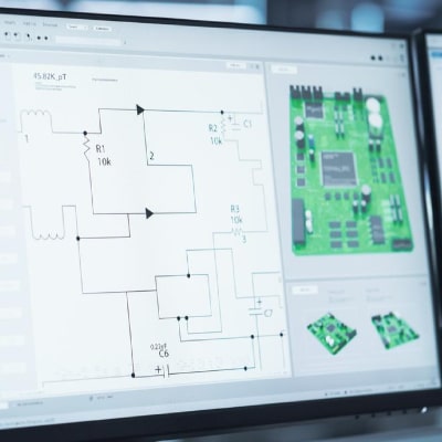

Schematic & Layout Design
Schematic Design
We help our customers to design schematic based on the high-level product requirements defined by an architect. We go through multiple reviews to achieve “Right First Time” approach, as our engineers are highly sensitive about the cost of HW iteration. We maintain a traceability matrix and the reviewer goes through the requirements so that the design is met with all the specified functionality. Our experienced team has the capability to design schematic of high-speed design with digital, analog, and Mixed-signal multilayer PCB.

PCB Layout
We have the capability of High-speed PCB layout for analog, digital, and mixed-signal boards for a variety of electronic systems and fields of application. We have experience in PCB design of Flex PCB, Rigid PCB and Mix (Flex+Rigid) PCB. Our team has experience in PCB design of HDI PCB with micro via, blind and buried via. We closely work with the mechanical engineer to make sure that the form factor fits into the targeted area. After a successful layout design, we took ownership to generate the Gerber file and resolve all engineering queries of the PCB manufacturing house for PCB fabrication and assembly.
Hardware Board Design
Hi-Speed Board Design
Engibrains offers a high-speed PCB design service that specializes in creating top-quality printed circuit boards that meet the needs of our clients. Our team of experienced engineers uses the latest design tools and techniques to ensure that each PCB design is optimized for high speed, low noise, and signal integrity.
Analog Board Design
We specialize in analog board design services that are tailored to the specific needs of our clients. Analog board design is a critical aspect of electronic systems that require precise analog signal processing, such as audio equipment, instrumentation, and control systems. Our team of experienced engineers has a deep understanding of analog circuitry and can design boards that meet the most demanding requirements.
Mixed-Signal Board Design
Mixed-signal board design involves creating a circuit board that can accurately process both analog and digital signals while minimizing noise and distortion. Our team of experienced engineers has a deep understanding of mixed-signal circuitry and can help you meet your design needs.
Hardware Architecture
Product Hardware Architecture
- We assist our customers in developing HW architecture based on their concept and desired targeted budget. Our in-depth experience and knowledge of various class A components from different vendors help you to finalize all class A components that suffice the concept, form factor, and budget.
- We have used SOC from Semiconductor companies like NXP, TI, Cypress, Dialog, STM, Nordic, Mediatek, Qualcomm, Renesas, Silicon Labs, Microchip, etc in our past projects.
Circuit Simulation
- As a part of the architecture process, we also finalized the BOM(Bill of Materials) that helps to get a pulse of the targeted cost of the HW before we went through the actual design.
- As a design house, we are associated with multiple class-A vendors including semiconductor giants. We always keep our eyes open for the new addition to the SOC portfolio, so we can serve the best fit to end customers.
Class-A BOM Identification
- As a part of the architecture process, we also finalized the BOM(Bill of Materials) that helps to get a pulse of the targeted cost of the HW before we went through the actual design.
- As a design house, we are associated with multiple class-A vendors including semiconductor giants. We always keep our eyes open for the new addition to the SOC portfolio, so we can serve the best fit to end customers.
Schematic & Layout Design
Schematic Design
We help our customers to design schematic based on the high-level product requirements defined by an architect. We go through multiple reviews to achieve “Right First Time” approach, as our engineers are highly sensitive about the cost of HW iteration. We maintain a traceability matrix and the reviewer goes through the requirements so that the design is met with all the specified functionality. Our experienced team has the capability to design schematic of high-speed design with digital, analog, and Mixed-signal multilayer PCB.
PCB Layout
We have the capability of High-speed PCB layout for analog, digital, and mixed-signal boards for a variety of electronic systems and fields of application. We have experience in PCB design of Flex PCB, Rigid PCB and Mix (Flex+Rigid) PCB. Our team has experience in PCB design of HDI PCB with micro via, blind and buried via. We closely work with the mechanical engineer to make sure that the form factor fits into the targeted area. After a successful layout design, we took ownership to generate the Gerber file and resolve all engineering queries of the PCB manufacturing house for PCB fabrication and assembly.
| Skill Matrix
Our Skill will reduce your risk
TOOLS
- Altium Designer
- Cadence OrCad
- Cadence OrCad pspice
- Cadence Allegro
- Mentor Graphics PADS
- Mentor Graphics hyperlynx
- CAM350
- SolidWorks
- LTspice
HW PLATFORM
- NXP Semiconductors
- Nordic Semiconductor
- Texas Instruments
- STMicroelectronics
- Renesas Electronics
- Infineon Technologies
- Espressif Systems
- Microchip Technology
- Ambiq
- Alif Semiconductor
- silabs
PERIPHERALS
- DDR3 / DDR4 RAM
- TFT Display
- Image Sensor
- eMMC/SD Flash
- eSIM
- 4G LTE
INTERFACES
- USB 3.1/3.0/2.0
- MIPI – CSI/DSI
- Octa SPI (High-Speed SPI)
- I3C (Next-Gen I2C)
- SPDIF/SAI (High-Speed Audio)
- SDIO/MDIO
- SSD/ SATA/Flash
- LVDS/HDMI/DVI
- Ethernet 10/100/1000
- WiFi 6.0/5.0/4.0
- Bluetooth 5.1/5.0/4.2/4.0
- WiFi/BLE Mesh
- Zigbee/Thread/NFC/LoRa


| Our Hardware Design Projects
Engineering marvels we delivered to market

Micro-object Detection System using Lens-Free Image Sensor

Industrial IOT – Digital Pressure Measurement Device

ANC+CVC Enabled Bluetooth 5.1 Neckband Development

ANC+CVC Enabled Bluetooth 5.1 Buds(TWS) Development

Workspace Utilization & Air Quality Monitoring System

In-Car Driver Safety System For Ride-share Segment
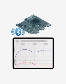
Low Current & Voltage Measurement Platform
| Lab Capability
Our QA engineers are well equipped with analysis & monitoring tools.

DMM6500 6½-Digit Digital Multimeterr
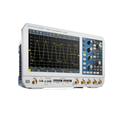
R&S®RTB2000 oscilloscopes

RSA306B USB spectrum signal analyzer
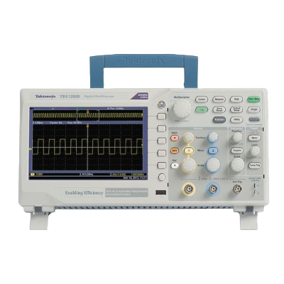
TBS1102B Digital Storage Oscilloscope

Aoyue 866 All in 1 Digital Hot Air Rework Station
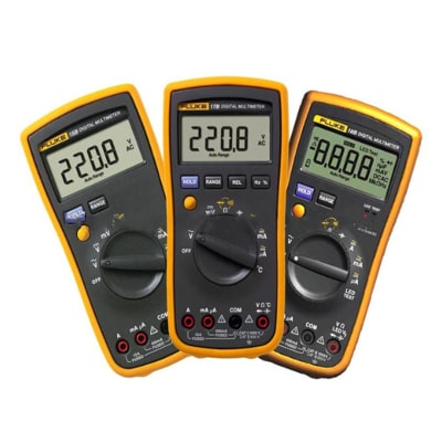
Fluke High-end Digital Multimeter

FLIR C5 Compact Thermal Camera

Tabletop 1080P Digital Microscope